

Infineon OPTIREG™ Mid-Range+ SBC - TLE9263BQX
- Availability: In Stock
- Free Shipping
- Shipping Time: 4~10 Business Days
-
$2.99
-
- 100 or more $2.50
- 500 or more $2.30
- 1000 or more $2.20
- 2000 or more $2.10
- 5000 or more $2.00
Body System IC with Integrated Voltage Regulators, Power Management Functions, HS-CAN Transceiver supporting CAN FD and Multiple LIN Transceiver. Featuring Multiple High-Side Switches and High-Voltage Wake Inputs.
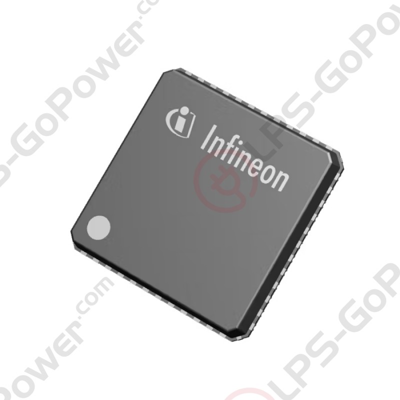
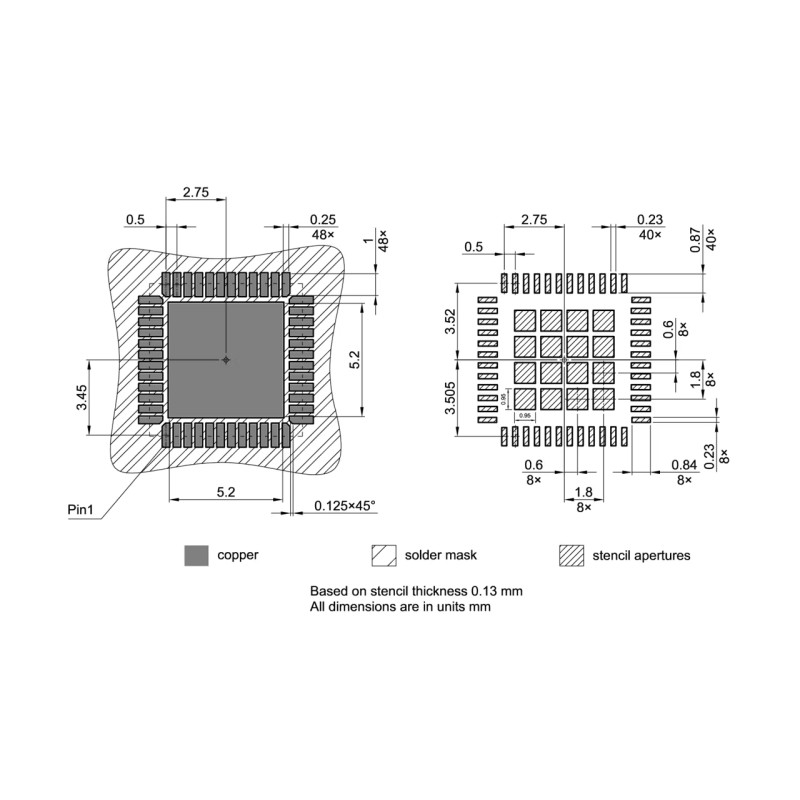
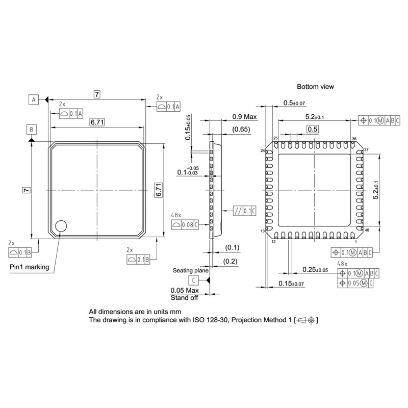
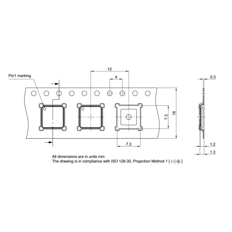
The TLE9263BQX is a monolithic integrated circuit in an exposed pad VQFN-48 (7 mm x 7 mm) power package with Lead Tip Inspection (LTI) feature to support Automatic Optical Inspection (AOI).
The device is designed for various CAN-LIN automotive applications as main supply for the microcontroller and as interface for a LIN and CAN bus network.
To support these applications, the System Basis Chip (SBC) provides the main functions, such as a 5 V low-dropout voltage regulator (LDO) for e.g. a microcontroller supply, another 5 V low-dropout voltage regulator with off-board protection for e.g. sensor supply, another 5 V/3.3V regulator to drive an external PNP transistor, which can be used as an independent supply for off-board usage or in load sharing configuration with the main regulator VCC1, a HS-CAN transceiver supporting CAN FD and LIN transceiver for data transmission, high-side switches with embedded protective functions and a 16-bit Serial Peripheral Interface (SPI) to control and monitor the device. Also implemented are a configurable timeout / window watchdog circuit with a reset feature, three Fail Outputs and an undervoltage reset feature.
The device offers low-power modes in order to minimize current consumption on applications that are connected permanently to the battery. A wake-up from the low-power mode is possible via a message on the buses, via the bilevel sensitive monitoring/wake-up inputs as well as via cyclic wake. The device is designed to withstand the severe conditions of automotive applications.
Features
- Two integrated Low-Drop Voltage Regulators: Main regulator with 5 V up to 250 mA (3.3 V variant available) and auxiliary regulator (5 V up to 100 mA) with off-board usage protection
- Voltage regulator (5 V or 3.3 V selectable ) with external PNP transistor configurable for off-board usage or for load sharing
- 1 high-speed CAN transceiver supporting FD communication up to 5 Mbit/s according to ISO 11898-2:2016 & SAE J2284 (Partial Networking option available)
- 2 LIN transceivers supporting LIN 2.2/ISO 17987-4/SAE J2602
- 4 high-side outputs 7 Ω typ., 2 HV GPIOs, 3 HV wake inputs
- Integrated fail-safe and supervision functions, e.g. fail-safe, watchdog, interrupt- and reset outputs
- 16-bit SPI for configuration and diagnostics
Potential applications
- Body Control Modules (BMC), Passive keyless entry and start modules, Gateway applications
- Heating, ventilation and air conditioning (HVAC)
- Seat, roof, tailgate, trailer, door and other closure modules
- Light control modules
- Gear shifters and selectors
Product validation
Qualified for automotive applications. Product validation according to AEC-Q100.
Parametrics
- Compatible Microcontrollers: TRAVEO™ T1G, T2G, AURIX™ TC2x, TC3x, PSOC™ 4x
- Family: OPTIREG™ Mid-Range+ SBC
- Output Drivers: 4 x High-Side Switch 150 mA
- Planned to be available until at least: 2039
- Quiescent Current: 15 µA (typ) Sleep Mode
- Standby Current: 44 µA (typ) Stop Mode
- Transceiver: 1 x CAN FD ISO 11898 - 2, 2 x LIN2.2 / J2602
- Transmission Rate max: 5 MBit/s
- Voltage Regulator Output ((VCC1)): 5V / 250 mA
- Voltage Regulator Output ((VCC2)): 5V / 100 mA
- Voltage Regulator Output ((VCC3)): 5V or 3.3V / up to 400 mA
- Wake-up Inputs: Wake Pins, CAN, LIN
| Type | Package | Marking |
|---|---|---|
| TLE9263BQX | PG-VQFN-48 | TLE9263BQX |